PakAlumni Worldwide: The Global Social Network
The Global Social Network
The West's Technological Edge in Geopolitical Competition
The US and its allies enjoy a significant technological advantage over China and Russia. The Chinese are working hard to catch up but the West is not standing still. It is making huge investments in research and development to maintain this edge as it becomes increasingly clear that the outcome of the ongoing international geopolitical competition will largely be determined by technology.
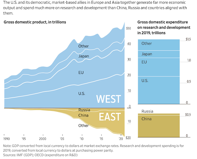 |
| East-West Comparison of GDP, R&D. Source: IMF (GDP), OECD (R&am... |
In 2019, the United States and its allies invested $1.5 trillion in research and development, far outpacing the combined Chinese and Russian R&D investment of half a trillion USD. This gap will likely narrow if the East's GDP continues to grow faster than the West's, allowing for higher investment in technology.
After the Russian invasion of Ukraine, the US, EU, Japan, South Korea and Taiwan have made it clear that the Western allies can and will use technology sanctions to control the behavior of China and Russia.
Taiwan Semiconductor Manufacturing Company (TSMC) will no longer fabricate computer chips for Russia, according to media reports. The ban will particularly affect Russia's Elbrus and Baikal processors, unless China agrees to step in to manufacture these chips, and risk additional US sanctions itself. Both Russian processors use mature 28 nm technology. The world's most advanced TSMC fabrication technology today is 5 nanometers. The best US-based Intel can do today is 7nm technology. China's SMIC (Semiconductor Manufacturing International Corporation) has the capability to produce chips using 14 nm technology. Semiconductor chips form the core of all modern systems from automobiles to airplanes to smartphones, computers, home appliances, toys, telecommunications and advanced weapons systems.
There is no question that the current western technology sanctions can seriously squeeze Russia. However, overusing such sanctions could backfire in the long run if the US rivals, particularly China and Russia, decide to invest billions of dollars to build their own capacity. This would seriously erode western technology domination and result in major market share losses for the US tech companies, particularly those in Silicon Valley.
Related Links:
Pakistani-American Banker Heads SWIFT, the World's Largest Interban...
Pakistani-Ukrainian Billionaire Zahoor Sees "Ukraine as Russia's Af...
Ukraine Resists Russia Alone: A Tale of West's Broken Promises
Ukraine's Lesson For Pakistan: Never Give Up Nuclear Weapons
Has Intel's Indian Techie Risked US Lead in Semiconductor Technology?
Views: 1602
-
Comment by Riaz Haq on August 8, 2025 at 10:16am
-
How Intel’s CEO Helped Create China’s Chip Industry - The Wall Street Journal.
https://www.wsj.com/tech/how-intels-ceo-helped-create-chinas-chip-i...
Over four decades and hundreds of investments, Tan’s U.S.-based venture-capital firm, Walden International, supported some of the biggest names in China’s chip industry. The list includes China’s leading chip manufacturer as well as smaller companies that filled essential niche roles.
At the time, most of the firm’s investments weren’t controversial, and many Silicon Valley venture capitalists and U.S. university endowments joined Tan in pouring billions of dollars into China.
With U.S.-China tensions now high, those investments no longer look so benign. Under both presidents Biden and Trump, Washington has restricted chip exports and chip-making equipment to China, fearing the military implications of Beijing’s technological advances.
In a statement, Tan said he shared the president’s “commitment to advancing U.S. national and economic security” and that Intel was working with the Trump administration “to address the matters that have been raised and ensure they have the facts.” He added that the U.S. has been his home for more than 40 years: “I love this country,” he said.
Tan was born in what is now Malaysia and raised in Singapore, where most of the population, like Tan, is of Chinese ancestry. The avid basketball player got a master’s degree in nuclear engineering from the Massachusetts Institute of Technology and a second master’s in business from the University of San Francisco. Now 65, he is a naturalized American.
Tan founded the San Francisco-based venture-capital firm Walden International in 1987 with the aim, he said decades later, of becoming “the pride of overseas Chinese.” Its name was inspired by the Henry David Thoreau book “Walden,” which championed simple living, self-sufficiency and contrarian thinking.
“I said, ‘I want to be an impact player and what can I offer?’ ” Tan recalled in a 2007 presentation at the University of California, Berkeley. He concluded that his background positioned him to bring U.S. investors to Asia and help Asian companies expand abroad.
In 1993, Chinese officials invited Walden to introduce the concept of venture capital to the Communist Party-run country, a company promotion video said. A year later, Walden established a China-focused fund.
Early investments went to both state-owned companies and China’s swelling class of entrepreneurs. At one point, it was the biggest shareholder in Sina, parent of Weibo , the Chinese social-media equivalent of X. “It is fair to say there would be no Sina today without Walden,” Sina’s chairman once said.
Tan’s impact was most profound in semiconductors. China remains behind its Asian rivals and the U.S. in major chip technologies, and while Intel’s principal competitors aren’t Chinese, they are catching up fast.
Walden was an early investor in SMIC, the company trying to become China’s answer to Taiwan Semiconductor Manufacturing , the widely recognized global leader in making cutting-edge chips. Although it still trails TSMC, SMIC is now China’s biggest chip maker.
Tan served on SMIC’s board of directors for at least 18 years. When the company went public on a Chinese exchange in 2020, Tan said that “Walden has stood alongside SMIC all the way” and supported its manufacturing breakthroughs.
Later that year, the Commerce Department took action to block SMIC from further breakthroughs and put it on a list restricting U.S. suppliers from selling equipment to the Shanghai-based company.
-
-
Bill Bishop
@niubi
Sounds like a massive security failure by ASML and the Dutch intelligence services - How China built its ‘Manhattan Project’ to rival the West in AI chips https://reuters.com/world/china/how-china-built-its-manhattan-proje...
https://x.com/niubi/status/2001326094428021157?s=20
------
Exclusive: How China built its ‘Manhattan Project’ to rival the West in AI chips
By Fanny Potkin
https://www.reuters.com/world/china/how-china-built-its-manhattan-p...
Shenzhen team completed a working prototype of a EUV machine in early 2025, sources say
The lithography machine, built by former ASML engineers, fills a factory floor, sources say
China's EUV machine is undergoing testing, and has not produced working chips, sources say
Government is targeting 2028 for working chips, but sources say 2030 is more likely
SINGAPORE Dec 17 - In a high-security Shenzhen laboratory, Chinese scientists have built what Washington has spent years trying to prevent: a prototype of a machine capable of producing the cutting-edge semiconductor chips that power artificial intelligence, smartphones and weapons central to Western military dominance, Reuters has learned.
Completed in early 2025 and now undergoing testing, the prototype fills nearly an entire factory floor. It was built by a team of former engineers from Dutch semiconductor giant ASML (ASML.AS), opens new tab who reverse-engineered the company's extreme ultraviolet lithography machines or EUVs, according to two people with knowledge of the project.
In April, ASML CEO Christophe Fouquet said that China would need "many, many years" to develop such technology. But the existence of this prototype, reported by Reuters for the first time, suggests China may be years closer to achieving semiconductor independence than analysts anticipated.
Nevertheless, China still faces major technical challenges, particularly in replicating the precision optical systems that Western suppliers produce.
The availability of parts from older ASML machines on secondary markets has allowed China to build a domestic prototype, with the government setting a goal of producing working chips on the prototype by 2028, according to the two people.
But those close to the project say a more realistic target is 2030, which is still years earlier than the decade that analysts believed it would take China to match the West on chips.
Chinese authorities did not respond to requests for comment.
The breakthrough marks the culmination of a six-year government initiative to achieve semiconductor self-sufficiency, one of President Xi Jinping's highest priorities. While China's semiconductor goals have been public, the Shenzhen EUV project has been conducted in secret, according to the people.
The project falls under the country's semiconductor strategy, which state media has identified as being run by Xi Jinping confidant Ding Xuexiang, who heads the Communist Party's Central Science and Technology Commission.
Chinese electronics giant Huawei plays a key role coordinating a web of companies and state research institutes across the country involving thousands of engineers, according to the two people and a third source.
The people described it as China's version of the Manhattan Project, the U.S. wartime effort to develop the atomic bomb.
“The aim is for China to eventually be able to make advanced chips on machines that are entirely China-made,” one of the people said. " China wants the United States 100% kicked out of its supply chains."
Huawei, the State Council of China, the Chinese Embassy in Washington, and China's Ministry of Industry and Information Technology did not respond to requests for comment.
Until now, only one company has mastered EUV technology: ASML, headquartered in Veldhoven, Netherlands. Its machines, which cost around $250 million, are indispensable for manufacturing the most advanced chips designed by companies like Nvidia and AMD—and produced by chipmakers such as TSMC, Intel, and Samsung.
-
-
Exclusive: How China built its ‘Manhattan Project’ to rival the West in AI chips
By Fanny Potkin
https://www.reuters.com/world/china/how-china-built-its-manhattan-p...
ASML built its first working prototype of EUV technology in 2001, and told Reuters it took nearly two decades and billions of euros in R&D spending before it produced its first commercially-available chips in 2019.
“It makes sense that companies would want to replicate our technology, but doing so is no small feat,” ASML told Reuters in a statement.
ASML's EUV systems are currently available to U.S. allies including Taiwan, South Korea, and Japan.
Starting in 2018, the United States began pressuring the Netherlands to block ASML from selling EUV systems to China. The restrictions expanded in 2022, when the Biden administration imposed sweeping export controls designed to cut off China's access to advanced semiconductor technology. No EUV system has ever been sold to a customer in China, ASML told Reuters.
The controls targeted not just EUV systems but also older deep ultraviolet (DUV) lithography machines that produce less-advanced chips like Huawei’s, aiming to keep China at least a generation behind in chipmaking capabilities.
The U.S. State Department said the Trump Administration has strengthened enforcement of export controls on advanced semiconductor manufacturing equipment and is working with partners "to close loopholes as technology advances.”
The Dutch Ministry of Defence said the Netherlands is developing policies requiring “knowledge institutions” to perform personnel screenings to prevent access to sensitive technology “by individuals that have ill intentions or who are at risk of being pressured.”
Export restrictions have slowed China's progress toward semiconductor self-sufficiency for years, and constrained advanced chip production at Huawei, the two people and a third person said.
The sources spoke on condition they not be identified due to the confidentiality of the project.
CHINA'S MANHATTAN PROJECT
One veteran Chinese engineer from ASML recruited to the project was surprised to find that his generous signing bonus came with an identification card issued under a false name, according to one of the people, who was familiar with his recruitment.
Once inside, he recognized other former ASML colleagues who were also working under aliases and was instructed to use their fake names at work to maintain secrecy, the person said. Another person independently confirmed that recruits were given fake IDs to conceal their identities from other workers inside the secure facility.
The guidance was clear, the two people said: Classified under national security, no one outside the compound could know what they were building—or that they were there at all.
The team includes recently retired, Chinese-born former ASML engineers and scientists—prime recruitment targets because they possess sensitive technical knowledge but face fewer professional constraints after leaving the company, the people said.
Two current ASML employees of Chinese nationality in the Netherlands told Reuters they have been approached by recruiters from Huawei since at least 2020.
Huawei did not respond to requests for comment.
European privacy laws limit ASML's ability to track former employees. Though employees sign non-disclosure agreements, enforcing them across borders has proven difficult.
ASML won an $845 million judgment in 2019 against a former Chinese engineer accused of stealing trade secrets, but the defendant filed for bankruptcy and continues to operate in Beijing with Chinese government support, according to court documents.
ASML told Reuters that it “vigilantly guards” trade secrets and confidential information.
"While ASML cannot control or restrict where former employees work, all employees are bound by the confidentiality clauses in their contracts," the company said, and it has "successfully pursued legal action in response to the theft of trade secrets.”
-
-
Exclusive: How China built its ‘Manhattan Project’ to rival the West in AI chips
By Fanny Potkin
https://www.reuters.com/world/china/how-china-built-its-manhattan-p...
Reuters was unable to determine if any legal actions have been taken against former ASML employees involved in China’s lithography program.
The company said it safeguards EUV knowledge by ensuring only select employees can access the information even inside the company.
Dutch intelligence warned in an April report that China "used extensive espionage programmes in its attempts to obtain advanced technology and knowledge from Western countries," including recruiting "Western scientists and employees of high-tech companies.”
The ASML veterans made the breakthrough in Shenzhen possible, the people said. Without their intimate knowledge of the technology, reverse-engineering the machines would have been nearly impossible.
Their recruitment was part of an aggressive drive China launched in 2019 for semiconductor experts working abroad, offering signing bonuses that started at 3 million to 5 million yuan ($420,000 to $700,000) and home-purchase subsidies, according to a Reuters review of government policy documents.
Recruits included Lin Nan, ASML's former head of light source technology, whose team at the Chinese Academy of Sciences' Shanghai Institute of Optics has filed eight patents on EUV light sources in 18 months, according to patent filings.
The Shanghai Institute of Optics and Fine Mechanics did not respond to requests for comment. Lin could not be reached for comment.
Two additional people familiar with China’s recruitment efforts said some naturalized citizens of other countries were given Chinese passports and allowed to maintain dual citizenship.
China officially prohibits dual citizenship and did not answer questions on issuing passports.
Chinese authorities did not respond to requests for comment.
INSIDE CHINA'S EUV FAB
ASML's most advanced EUV systems are roughly the size of a school bus, and weigh 180 tons. After failed attempts to replicate its size, the prototype inside the Shenzhen lab became many times larger to improve its power, according to the two people.
The Chinese prototype is crude compared to ASML's machines but operational enough for testing, the people said.
China's prototype lags behind ASML's machines largely because researchers have struggled to obtain optical systems like those from Germany's Carl Zeiss AG, one of ASML's key suppliers, the two people said.
Zeiss declined to comment.
The machines fire lasers at molten tin 50,000 times per second, generating plasma at 200,000 degrees Celsius. The light is focused using mirrors that take months to produce, according to Zeiss' website.
China's top research institutes have played key roles in developing homegrown alternatives, according to the two people.
The Changchun Institute of Optics, Fine Mechanics and Physics at the Chinese Academy of Sciences (CIOMP) achieved a breakthrough in integrating extreme-ultraviolet light into the prototype's optical system, enabling it to become operational in early 2025, one of the people said, though the optics still require significant refinement.
CIOMP did not respond to requests for comment.
In a March online recruitment call on its website, the institute said it was offering "uncapped" salaries to PhD lithography researchers and research grants worth up to 4 million yuan ($560,000) plus 1 million yuan ($140,000) in personal subsidies.
Jeff Koch, an analyst at research firm SemiAnalysis and a former ASML engineer, said China will have achieved "meaningful progress” if the “light source has enough power, is reliable, and doesn’t generate too much contamination.”
"No doubt this is technically feasible, it's just a question of timeline," he said. "China has the advantage that commercial EUV now exists, so they aren't starting from zero."
-
-
Exclusive: How China built its ‘Manhattan Project’ to rival the West in AI chips
By Fanny Potkin
https://www.reuters.com/world/china/how-china-built-its-manhattan-p...
To get the required parts, China is salvaging components from older ASML machines and sourcing parts from ASML suppliers through secondhand markets, the two people said.
Networks of intermediary companies are sometimes used to mask the ultimate buyer, the people said.
Export-restricted components from Japan’s Nikon and Canon are being used for the prototype, one of the people and an additional source said.
Nikon declined to comment. Canon said it was not aware of such reports. The Japanese Embassy in Washington did not respond to a request for comment.
International banks regularly auction older semiconductor fabrication equipment, the sources said. Auctions in China sold older ASML lithography equipment as recently as October 2025, according to a review of listings on Alibaba Auction, an Alibaba-owned platform.
A team of around 100 recent university graduates is focused on reverse-engineering components from both EUV and DUV lithography machines, according to the people.
Each worker's desk is filmed by an individual camera to document their efforts to disassemble and reassemble parts—work the people described as key to China's lithography efforts.
Staffers who successfully reassemble a component receive bonuses, the people said.
HUAWEI SCIENTISTS SLEEP ON-SITE
While the EUV project is run by the Chinese government, Huawei is involved in every step of the supply chain from chip design and fabrication equipment to manufacturing and final integration into products like smartphones, according to four people familiar with Huawei’s operations.
CEO Ren Zhengfei briefs senior Chinese leaders on progress, according to one of the people.
The U.S. placed Huawei on an entity list in 2019, banning American companies from doing business with them without a license.
Huawei has deployed employees to offices, fabrication plants, and research centers across the country for the effort. Employees assigned to semiconductor teams often sleep on-site and are barred from returning home during the work week, with phone access restricted for teams handling more sensitive tasks, according to the people.
Inside Huawei, few employees know the scope of this work. "The teams are kept isolated from each other to protect the confidentiality of the project," one of the people said. “ They don't know what the other teams work on.”
Comment
- ‹ Previous
- 1
- …
- 7
- 8
- 9
- Next ›
Twitter Feed
Live Traffic Feed
Sponsored Links
South Asia Investor Review
Investor Information Blog
Haq's Musings
Riaz Haq's Current Affairs Blog
Please Bookmark This Page!
Blog Posts
Pakistan Needs to Address Its Significant Data Quality Challenges
Policy-makers need data to formulate good policies. Good data produced by government agencies can be expected to lead to good policies and desirable outcomes. But data collection and statistical analyses require adequate methodologies and resources. Unfortunately, Pakistan's data quality gets a "C" grade by international agencies like the International Monetary Fund (IMF). Clearly the country faces significant data quality challenges. These challenges range from estimation of the size…
ContinuePosted by Riaz Haq on July 7, 2026 at 9:30am — 8 Comments
Pakistan Electricity Consumption Up 21% in Just Two Years
Pakistan is experiencing soaring demand for electricity across all of the sectors of its economy. The new demand is being met by rapidly growing deployment of distributed solar, estimated at 38 GW as of June, 2025. In 2025, 44% of solar deployment was residential, followed by industry (26%), agriculture (21%) and commercial users (9%). The expansion of distributed solar has enhanced electrification across the economy, lifting Pakistan's electrification rate to 21.7%…
ContinuePosted by Riaz Haq on June 30, 2026 at 1:30pm — 7 Comments
© 2026 Created by Riaz Haq.
Powered by
![]()
You need to be a member of PakAlumni Worldwide: The Global Social Network to add comments!
Join PakAlumni Worldwide: The Global Social Network